Prof. YE Jichun’s team at the Ningbo Institute of Materials Technology and Engineering (NIMTE) of Chinese Academy of Sciences (CAS), cooperating with researchers at the University of Nottingham Ningbo China, has revealed the underlying dynamics of Silicon oxide (SiOx) tunneling junctions, including pinhole formation processes and charge-carrier transport mechanisms. The study was published in Cell Reports Physical Science.
As one of the most promising alternatives to reduce the cost and improve the efficiency of devices, Tunnel Oxide Passivating Contact (TOPCon) technology has recently attracted considerable attention in the photovoltaic (PV) community. However, the physical mechanism of the core structures of TOPCon, i.e., polycrystalline silicon (poly-Si)/ SiOx/ crystalline silicon (c-Si) junctions, are not yet fully clarified, thus restricting the further improvement of device efficiency.
To address this problem, researchers at NIMTE conducted extensive experiments and simulations, unraveling the underlying charge carrier dynamics of the SiOx tunneling junctions.
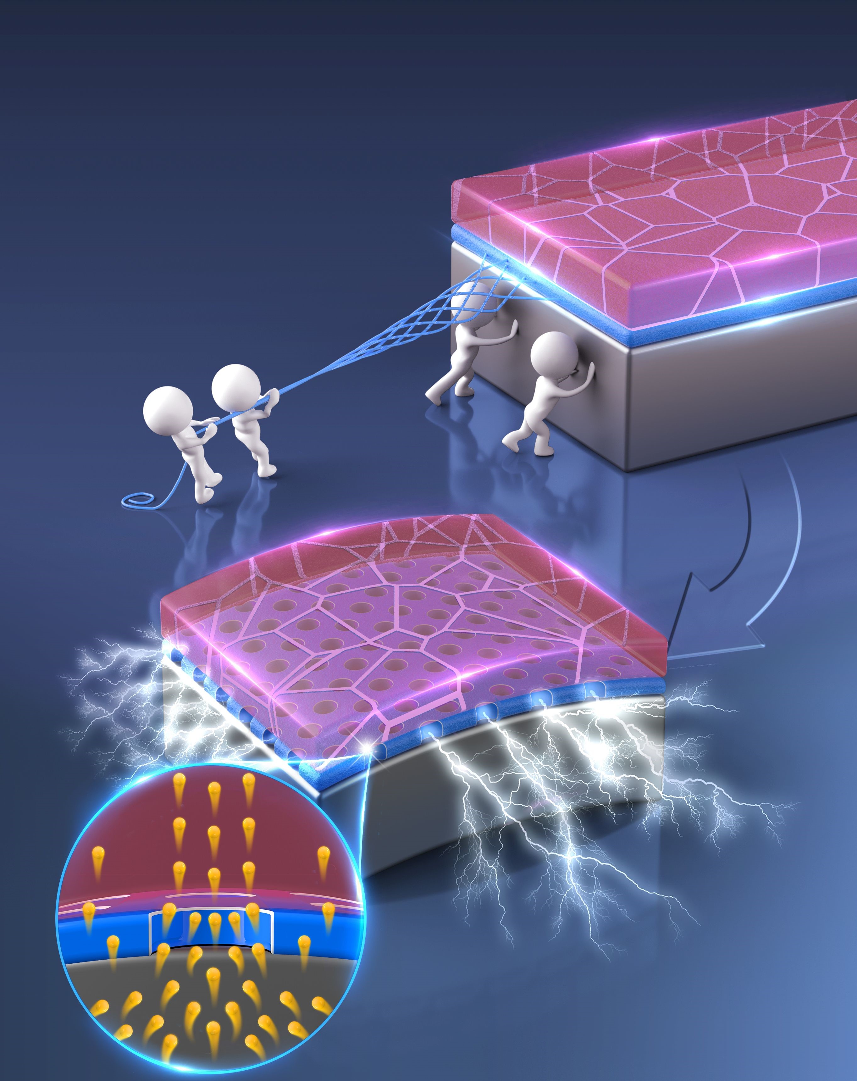
By virtue of refined experiments, the pinhole formation process was revealed, suggesting that interface stress induced by the mismatch of thermal expansion coefficients during at high temperatures may account for the fracture of SiOx films.
In addition, the simulation results provided direct evidence for charge carrier transport theory, demonstrating that tunneling charge-carrier transport functions in tandem with direct transport through pinholes. Which mechanism plays the dominant role depends on the density and size of pinholes as well as the SiOx thickness.
Furthermore, a fundamental physical model with local pinholes was developed with the simultaneous consideration of the passivation and contact behaviors. A detailed current-recombination analysis in conjunction with predictions of device efficiency showed that the potential device efficiency can reach 27%.
The results demonstrated in this study concerning the pinhole formation and charge carrier transport mechanisms, could not only shed new light on the underlying device physics of poly-Si/SiOx/c-Si junctions, but also offer valuable guidance to unlock the full potential for high-efficiency TOPCon device design, which is crucial to both academia and industry.
This work was supported by the Key Research and Development Program of Zhejiang Province (No. 2021C01006), National Key R&D Program of China (Grant No. 2018YFB1500403), National Natural Science Foundation of China (Nos. 61974178, 61874177, 62004199), Ningbo “Innovation 2025” Major Project (No. 2020Z098), Youth Innovation Promotion Association (No. 2018333), Zhejiang Provincial Natural Science Foundation (No. LY19F040002).

Fig. Schematic diagram of the pinhole formation and charge-carrier transport (Image by NIMTE)
Contact
YANG Zhenhai
Ningbo Institute of Materials Technology and Engineering
E-mail: yangzhenhai@nimte.ac.cn

