Metamaterials are artificially engineered to have properties that are not earned in nature. They are made from assemblies of composite materials,in which the repeating patterns are always involved. Metamaterials possess novel properties not coming from the properties of the base materials, but from their newly designed microstructures, i.e., their shape, geometry, size, orientation, and spatial arrangement do contribute to the new-born properties by blocking, absorbing, enhancing, or bending electromagnetic waves, to achieve man-made benefits eventually.
As well known, electrochemical deposition methods are very popular to fabricate anisotropic meta-surfaces and metamaterials, among which AAO (anodic aluminum oxide) template-assisted preparation is a representative example. However, on one hand, there are some unbridgeable disadvantages in such technique; one the other, it is still a real problem for unskilled green hands. Now a convenient template-free preparation method is proposed that is appealing for material scientists.
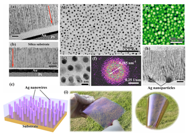
Dr. Junhua Gao, Prof. Hongtao Cao, Prof. Yinglin Song and co-authors from Ningbo Institute of Materials Technology & Engineering, Chinese Academy of Sciences and Harbin Institute of Technology have demonstrated the direct growth of vertically-aligned silver nanoforest embedded-ceramic composite films with tunable optical responses.
With the aid of radio frequency (RF) substrate bias-assisted sputtering deposition, dense ultrafine Ag nanowire array (namely, nanoforest) embedded-ceramic metamaterial films were directly prepared near room temperature, with an average diameter of ~3 nm and well-defined sub-5 nm inter-wire spacing. The geometric structure of the nanoforest (such as nanowire diameter, length, and inter-wire spacing) could be flexibly tuned by setting different sputtering parameters. The approach is independence of single-crystal or conducting substrates, practicable on flexible substrates, and easy to scale up. More interestingly, in analogy with building up N-floor mansion, multi-layer-stacked structures are also easily fabricated by vertical integration of different single-layer metamaterial films.
During the directional growth, three processes are involved: site-specific migration of Ag adatoms and addressing accumulation on the already-existed Ag lattice facets; Ag adatoms stack along a certain direction and dominated growth; preferential etching of Ag adatoms in high energy surfaces.

Intriguing steady and transient optical responses in the nanoforest assemblies are demonstrated, owing to their nanoscale structural anisotropy. The proposed method would provide an extensible material preparation platform to make new structures and manipulate optical response in the region of sub-5 nm scale. As continuously promoting, it can be potentially used in the field of nanophotonics, metamaterial-based electromagnetic manipulation, sub-wavelength imaging, and so on.
The material preparation method has been applied for Chinese invention patent protection, and the above-mentioned academic results have been published on Advanced Materials, 2017, DOI: 10.1002/adma.201605324.
The authors are grateful for the financial support from the National Nature Science Foundation of China, the Natural Science Foundation of Zhejiang Province, the Key Laboratories of Zhejiang Province, and the program for Ningbo Municipal Science and Technology Innovative Research Team.
Prof. Dr. Hongtao Cao: h_cao@nimte.ac.cn
All images by ![]()

