The explosive increment of information in the era of big data has raised the demand of low power consumption, miniaturization and multifunction integration for the electronic devices to process and store the massive data more efficiently. However, due to the separation of the processing and memory units in the conventional von Neumann architecture, the computers have to consume vast amount of CPU cycles to fetch and shuttle data in the various levels of memory hierarchy, and are only capable to executing the demands and computing tasks one-by-one, therefore limiting parallel processing capability of the state-of-the-art computer systems with substantial latency and energy costs. The research team led by Prof. Run-Wei Li at the Key Laboratory of Magnetic Materials and Devices (Ningbo Institute of Materials Technology and Engineering, Chinese Academy of Sciences) have devoted great efforts on the prospective investigation of tuning the resistance and magnetism of the storage medium by multiple physical fields to develop novel information storage mode and to enhance the extent of functionality integrity of the devices in recent years.
Generally, the integration of multi-photonic-functionalities, including the on-chip sources, manipulators, filters, multipliers, detectors and storage, into microelectronic platforms, has been considered as an alternative solution for the size-scaling and intellectualization campaign of the post-Moore era to co-perform the coding, transfer, decoding, computing, processing and storage operation of the information. An important module of such optoelectronic integrated circuits would be the field-induced resistive switching memory, the major task of which is to write and store the electrical bits of information through optical means. Additional merits of the communication and computation capabilities may also lower the complexicity of the integrated circuits, and make them more proficient when dealing with the rapidly increased massive data generated nowadays. Very recently, Mr. Hongwei Tan and Dr. Gang Liu from Prof. Li’s groups demonstrated that persistent and electrically-erasable photoconductance can be realized in the broadband UV-Visible spectrum with linear relationship to the illumination time, based on the optical and electrical dual-control of the trapped electron density at the interface of the CeO2-x/AlOy/Al Schottky contact. Consequently, they constructed an optoelectronic resistive switching memory (OE-Memory) with integrated demodulating and arithmetic functions, composed of an ITO/CeO2-x/AlOy/Al junction structure, for future information technology. For instance, the intensity- and wavelength-dependent resistances of the device can be used to demodulate the broadband optical information into electrical signals, while the stepwise and linear response of the photocurrent makes the device capable of performing counting and arithmetic operations. Moreover, the received optical digital signals can be stored non-volatilely by the multilevel and persistent photoresponses of the device, thus providing considerable potential for non-volatile optoelectronic memory devices with higher information storage and processing capacity. Related results have been filed into a Chinese patent (201510114334.6), as well as published on Advanced Materials as the back cover article.

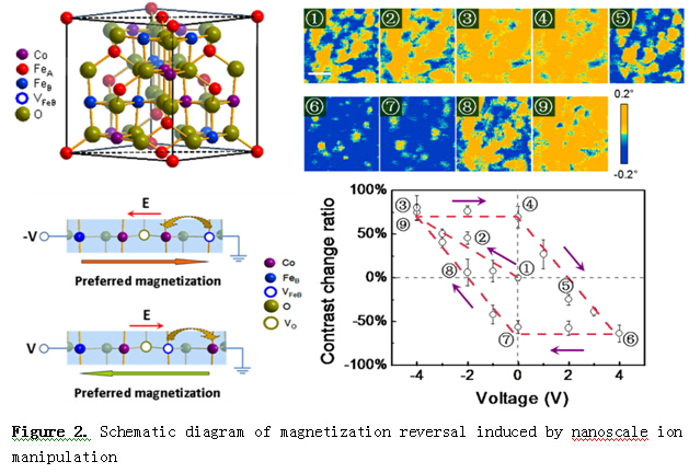
On the other hand, magnetic storage has been a mainstream player of the field for decades. Regardless the choice of conventional magnetic hard disk or novel magnetic random access memory, external magnetic field or electric current is usually used to write the information, which is unfavored for the miniaturization and low-power consumption requirement of the devices. Therefore, to realize the controlling of nanoscale magnetization by electric field has become a research hotspot in the past ten years. In cooperation with Prof. Jun Ding from the National University of Singapore, Ms. Xinxin Chen, Dr. Xiaojian Zhu and Dr. Gang Liu have proposed that electric field-induced migration and local redistribution of the ions can be employed to modulate the magnetization of ferrite thin films. Through first-principle calculation, it was found that the Co2+ ions adjacent to the B-site Fe3+ vacancies are capable of migrating and being redistributed under electric field to induce unidirectional magnetic anisotropy in the (110)-textured CoFe2-xO4 (CFO) thin films with Fe vacancies. Consequently, by using the scanning probe technique to apply biased voltage onto the CFO thin films in nanoscale and observed the revolution of the local magnetic domains in situ, it is demonstrated that magnetization reversal can be achieved at room temperature via electrical ion-manipulation with low power consumption characteristics. Without the assistance of an external magnetic field, the present strategy of utilizing electric field-induced migration and redistribution of ionic species to modulate the nanoscale magnetization at room temperature is considered more favorable for the construction of novel spintronic devices. Related results have been published on ACS Nano.

Prof. Runwei Li: runweili@nimte.ac.cn
Mr.Hongwei Tan:tanhongwei@nimte.ac.cn
Research Staff Url:
http://english.nimte.cas.cn/rh/rd/newmaterials/mmd/mmd_research_interests/
All Images by ![]()

