With the development of three dimensions (3D) nanostructured devices such as information storage, biomimetic smart materials, metamaterials, and micro-electromechanical system (MEMS) devices, 3D micro/nanofabrication technology has received increasing attention.
Among the 3D microfabrication technologies that are compatible with electronic devices, e-beam-based or focused ion beam-based deposition and direct writing with metal colloidal ink have been explored as methods for fabricating 3D interconnects with micro- or nanoscale dimensions. The process for the former two methods needs to be performed in a high-vacuum environment and the deposited metals tend to have low electrical quality. Direct writing has been used to fabricate wire bonds ~10 µm in diameter and the finite size of the colloidal particles limits the minimum nozzle size that can be used to dispense the colloidal dispersion.
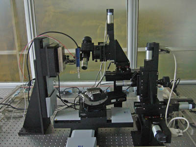
Recently, Prof. GaojieXu’s group from the Ningbo Institute of Materials Technology and Engineering (NIMTE), CAS has successfully manufactured a direct-writing 3D micro/nano wire bonds manufacturing system with Prof. MinfengYu, his partner from the Georgia Institute of Technology, USA. The automated system exploits micro or nanoscale liquid meniscus to electrodeposit metals, conductive polymers, and semiconductors with 3D micro/nano-structures of designed shapes in an ambient air environment.

Fig. 1 Photograph of the direct-writing 3D micro/nanowire bonds manufacturing system
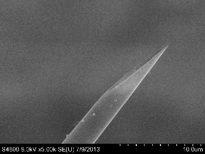
The meniscus-confined 3D electrodeposition relies on an electrolyte-containing micropipette with a microscopic dispensing nozzle (several micrometers down to 100 nm in diameter) as the working toolbit. As the micropipette approaches a conductive substrate surface, a meniscus is established between the dispensing nozzle and the substrate surface. With an appropriate electrical potential applied between the electrolyte contained in the micropipette and the substrate surface, electrodeposition is initiated within the substrate surface confined by the meniscus.

Fig. 2 SEM image of the nozzle at the end of a glass micropipette
The key to fabricating the interconnect is to synchronize the withdrawal speed of the micropipette away from the substrate surface with the growth rate of the local deposit, which maintains the stable formation of the meniscus now established between the nozzle and the growth front of the deposited wire, thereby sustaining the continuous growth of the off-surface micro- or nanowires. The method thus represents an advance over technologies such as electrochemical dip-pen lithography, in which the deposition is limited to surface patterning or electric field–enhanced electrodeposition with a sharpened metal tip, and the local electro- deposition is realized through the localization of the electric field near the end of the tip and fabrication must be performed with both the work piece and the tip immersed in an electrolyte environment.
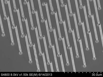
This technology is intrinsically capable of fabricating wires down to nanometer sizes, because the diameter of the deposited wire is defined by the size of the nozzle. Prof. Xu’s team has grown the array of Cu wires with ~100 nm in diameter using the technology. Compared with conventional electrodeposition technologies, its growth rate (> 1.3 µm/s) has several orders of magnitude increment. The approach is available for fabricating high-frequency terahertz antenna (high aspect ratio >100), precision sensors, and so on, based on the above advantages. More importantly, the equipment can allow the mass production of 3D micro- and nanostructures assisted by the micropipette array.
This technology is intrinsically capable of fabricating wires down to nanometer sizes, because the diameter of the deposited wire is defined by the size of the nozzle. Prof. Xu’s team has grown the array of Cu wires with ~100 nm in diameter using the technology. Compared with conventional electrodeposition technologies, its growth rate (> 1.3 µm/s) has several orders of magnitude increment. The approach is available for fabricating high-frequency terahertz antenna (high aspect ratio >100), precision sensors, and so on, based on the above advantages. More importantly, the equipment can allow the mass production of 3D micro- and nanostructures assisted by the micropipette array.

Fig. 3 SEM image of an array of Cu wire fabricated by the direct-writing manufacturing system
Prof. Gaojie Xu xugj@nimte.ac.cn
Research Group Url: http://english.nimte.cas.cn/rh/rd/mnfma
All Images by 

