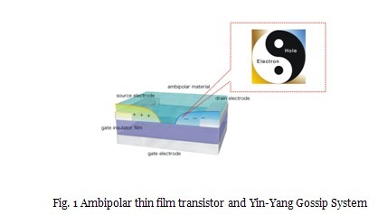
To date, a distinct nature of almost all the reported oxide semiconductor-based transistors is that they transport only a single carrier type, either electrons (n-type) or holes (p-type). Thus, simultaneous or controllable transport of electrons and/or holes (ambipolar charge transport, see Fig. 1, electron and hole resemble the Yin and Yang gossip system) is highly desirable, because it could enable the design of new-generation complementary non-Si-based electronic circuits as well as the construction of multi-functional devices such as light-emitting, light-sensing, and light-detecting transistors, i.e., one can integrate brand-new functionalities into the conventional transistor that is only a dissipative charge transporting device.
In addition, ambipolar thin film transistors with thereby simplified circuit design and fabrication processes (No separate patterning or/and doping steps needed) can reduce the complexity of device and circuit processing to the minimum.

In an ambipolar transistor, both the hole and electron are injected effectively into the channel and then manipulated by the polarity of the electrostatic potential to move through it. To construct high performance ambipolar transistors, one of the challenges lies in the efficient and balanced injection of both carriers from the source/drain (S/D) electrodes into a single channel layer (Fig. 2b), depending on the selection of a channel with small band-gap and proper band alignment between the S/D electrodes and semiconductor channel contact; and the other, the mother channel should have good conductivity for both carriers.
So far, however, research of oxide semiconductor-based ambipolar devices has hindered by materials difficulties. For example, oxide semiconductors with excellent performance are almost n-type and there are a few p-type oxides suitable for electronic devices, because hole transport is restricted in oxide semiconductors due to their deep valence band maximum (VBM) composed of 2p orbitals of oxygen ions with strong directivity and large electronegativity.
To circumvent the challenge, Tin mono-oxide (SnO) thin films were selected as the ambipolar transistor channel. SnO with litharge-type layered structure has been confirmed to be a appreciate p-type semiconductor because of its Sn 5s nature near the VBM. Dr. Hongtao Cao’s group already reported that SnO exhibited a reasonably high hole Hall mobility of ~ 3.9 cm2V-1s-1 at room temperature, and successfully fabricated SnO-based p-channel TFTs. Most importantly, their previous studies have revealed a fundamental but attractive property of SnO, i.e., it has a large direct optical band-gap of ~2.7 eV despite a small fundamental band-gap of ~ 0.5 eV. In principle, the wide optical band-gap of SnO preserves rather high transparency in the visible region, while the small band-gap favors the ambipolar behavior.
Dr. Lingyan Liang, Dr. Hongtao Cao, and their collaborators examined SnO for the properties of ambipolar channel for use in the oxide-based electronics (Appl. Phys. Lett., 100, 263502(2012)).

Shown in the insert of Fig. 2a is a schematic of a top-contact and bottom-gate (TC-BG) TFT with the polycrystalline SnO, Ni/Au (50/30 nm) and SiO2 (106 nm) as the channel, source/drain electrode and gate dielectric, respectively. The measured output characteristics exhibit a typical ambipolar feature that the type of accumulated carriers depends on the magnitude and polarity of gate (VG) and drain (VDS) voltages. Near symmetric characteristics between n- and p-type operations were unambiguously observed. A saturation field-effect mobility (μsat) of ~0.16 cm2V-1s-1 and linear field-effect mobility (μlin) of ~0.32 cm2V-1s-1 for p-channel and ~0.63 cm2V-1s-1 (μsat) and ~1.02 cm2V-1s-1 (μlin) for n-channel operation were obtained, manifesting that the injection and transport of holes are comparable to those of the electrons.
The balanced ambipolar feature of SnO TFTs favors to construct CMOS-like inverters using two identical (the same geometry and dimension, and shown in Figure 3a) transistors with a common gate as the input voltage VIN. The voltage transfer characteristics (VTCs) at different supply voltages (VDD) are presented in Fig. 3b, where the typical and comparable ambipolar inverter behaviors are seen in the first (positive VDD and VIN) and third quadrants (negative VDD and VIN). The extracted voltage gain is measured to be 30.6 (VDD = 40 V) and 31.3 (VDD = -40 V) in the first and third quadrants, respectively (Fig. 3c), which are comparable to those of the ambipolar inverters containing different channel materials such as microcrystalline silicon and organics. This feature, combined with a good logic voltage swings (> 82% of the highest output voltage) and wide noise margins (~20%), demonstrates that the SnO-based ambipolar inverter could be a robust building block of logic circuits for large area oxide electronics.

Prior to the paper publication, the relevant patent on SnO-based ambipolar transistors and inverters has been registered (No. 201210040980.9). Earlier on, two patents from our group on SnO material’ preparation (ZL200910152532.6) and p-type transistor (ZL201010040097.0) had been authorized.
The related work is supported by the Chinese National Program on Key Basic Research Project, the National Natural Science Foundation of China, and the Science and Technology Innovative Research Team of Ningbo Municipality, etc.
Images by NIMTE
Professor Hongtao Cao h_cao@nimte.ac.cn
Research Group Url: http://english.nimte.cas.cn/rh/rd/mstffd/

