Progresses of p-type SnO Film and Research of Its Electronics Devices
TFTs based on transparent oxide semiconductors (TOSs) such as zinc oxide (ZnO), tin dioxide (SnO2), indium-zinc oxides (IZO), indium-gallium-zinc oxide (IGZO)and other transparent oxides have attracted considerable research attention on basis of their good transparency, high field-effect mobility, making them possible to replace amorphous and poly-silicon in the area of the flat panel display and have potential applications in transparent flexible electronics due to low thermal budget. However, most of high mobility oxide semiconductors show n-type conduction; only a limited number of oxides exhibit p-type conduction with acceptable Hole mobilities. Thus, applications of oxide semiconductor TFTs has been limited to n-channel ones.
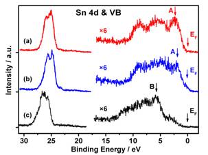
Recently, SnO has attracted attention simply because it exhibits an advantage of high Hole mobility in p-type oxide devices. It has been proposed that the valence band maxima (VBM) of SnO was mainly contributed by Sn 5s orbitals. Isotropic extended s orbitals constitute largely overlapped wave functions of the cations, which forms effective carrier conduction paths, thus, SnO exhibits a fairly high Hole mobility among p-type semiconductor oxides. Moreover, the p-type conductivity of SnO was suggested to originate from the tin vacancy, and it can be further improved via proper doping. Those properties make SnO a promising candidate to be a new p-type oxide semiconductor utilized for novel applications in areas such as photovoltaics, electronics, displays, sensors, information storage, etc.
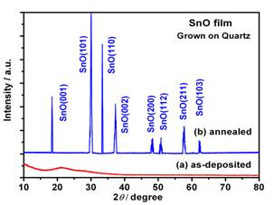
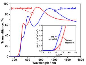
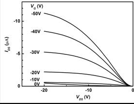
A simple, low cost two-step method was proposed for preparing single phase SnO polycrystalline thin films on quartz glasses. X-ray diffraction (XRD) analysis revealed that the annealed films were consisted of polycrystalline α-SnO phase without preferred orientation, and their single phase in nature was testified by chemical composition analysis using X-ray photoelectron spectroscopy (XPS). Transmittance spectra in UV-vis-IR range presented that the average transmittance was 70%, for both the as-deposited and annealed films. Especially, the optical band gap decreased from 3.20 to 2.77 eV after annealing process, which was ascribed to the crystalline size related quantum size effect. Moreover, the p-type conductivity of SnO film was confirmed by Hall effect measurement, with a Hall mobility of 1.4 cm2 V−1 s−1 and a hole concentration of 2.8 ×1016 cm−3. Moreover, Bottom-gate type thin film transistors (TFTs) employing polycrystalline α-SnO channels on the SiO2/Si(001) substrates exhibited p-type field-effect transistor characteristics. The optimum field-effect mobilities μsat and μlin are 0.46 cm2 V−1 s−1 and 0.87 cm2 V−1 s−1, respectively. The above-mentioned results have been published [1. ACS Appl. Mater. Interfaces, 2010, 2, 1060. 2. Appl. Phys. Lett., 2010, 96, 042113 (Joint paper with Prof. Pan’s group ) 3. ACS Appl. Mater. Interfaces, 2010, 2, 1565. 4. J. Electrochem. Soc., 2010, 157, H598]
The authors from Prof. Hongtao Cao’s group are grateful for the financial supports of the key project of the Natural Science Foundation of Zhejiang province (Grant No.Z4080347), Qianjiang Talent Program of Zhejiang Province (Grant No. 2009R10072), the CAS/SAFEA International Partnership Program for Creative Research Teams, the aided program for Science and Technology Innovative Research Team of Ningbo Municipality (2009B21005), and Special Foundation of President of the Chinese Academy of Sciences (Grand No. 080421WA01).


Figure1 XRD patterns of SnOx Figure 2. Transmittance spectra of
the SnO samples


Figure 3 The valance band of SnO and SnO2. Figure 4 The output curves of SnO-based TFT.

